Lab 03: Logic Gates
Objective
- Understand and experiment with basic logic gates (NOT, AND, OR, NAND, NOR, XOR, XNOR).
- Learn to construct and analyze circuits using these gates.
- Verify the functionality of these logic gates through truth tables and circuit testing.
- Use an oscilloscope to observe signal behavior in logic gates.
- Apply binary counting and logic gate connections in practical experiments.
Required Reading Materials
- Textbook: Digital Design: with an introduction to the Verilog HDL, 5th edition, Mano and Ciletti, ISBN-13: 978-0-13-277420-8
Chapter 2 - Datasheet: 7400, 7402, 7404, 7408, 7432, 7486, 7493, 7410
Components Required
| Component/Device | Description | Quantity |
|---|---|---|
| 7400 Quad 2-input NAND | × 1 | |
| 7402 Quad 2-input NOR | × 1 | |
| 7404 Hex Inverters (NOT) | × 1 | |
| 7408 Quad 2-input AND | × 1 | |
| 7410 Triple 3-input NAND | × 1 | |
| 7432 Quad 2-input OR | × 1 | |
| 7486 Quad 2-input XOR | × 1 | |
| 7493 4-bit Ripple Counter | × 1 |
Experiments
Every experiment section that requires you to build a circuit and test it has an asterisk (*). For those sections:
- For the in-class lab: Demonstrate the working circuit to your lab instructor.
- For online lab: Take a video to describe your circuit, upload the video to YouTube, and put the link in the report.
Exp #3.1 Basic Logic Functions
Basic Logic Functions
There are three basic logic functions from which all circuits can be designed: NOT (invert), OR, and AND. In addition, another useful logic function is exclusive-OR or XOR.
The NOT function is also known as INVERT (so a NOT gate is also called an INVERTER, as explained in Lab 01). The NOT function is true (1) if the input is false (0) and vice versa. The logical expression for the inverse of logic variable X is X (i.e., NOT X).
The logic gate symbol of a NOT/INVERTER is shown below. The triangle without the bubble at the output is called a "buffer gate". It does not change the gate's logic level. Instead, for the same logic level, it may output a load much more current than its input source is capable of.

It is the bubble at the end of the gate that indicates inversion. The bubble on the output of any gate means that the output level generated inside the gate is complemented before it appears at the actual gate output.
The AND function is true (1) only if all inputs are true (1s). The NAND function is an AND-NOT function and the inverse of an AND function. So, a NAND function is false (0) if all inputs are true (1s). Conversely, it is true (1) if one or more inputs are false (0). The logical expression for the AND of two variables, X and Y, is X•Y (or XY). The logical expression for the NAND of X and Y is (X•Y) or (XY). The symbol for a NAND is the same as for an AND except for a bubble at the end (as shown below). So if the inputs to a NAND are all 1s, the internal AND function produces a 1, which is then inverted to a 0 by the bubble.
The OR function is true (1) if one or more inputs are true (1). The NOR function is an OR-NOT function and inverse of an OR function. So, a NOR function is false (0) if one or more inputs are true (1). Conversely, it is true (1) only if all inputs are false (0s). The logic equation for the OR of two logic variables, X and Y, is X+Y. The logic equation for the NOR of X and Y is (X+Y).
The 2-variable (2-input) XOR function is true (1) if either input is true (1) but not both. The XOR is known as an odd function. If an odd number of its inputs are true (1), the output is true (1) – this definition works for any number of inputs. An XNOR is an XOR-NOT function. For a 2-variable (2-input) XNOR function, the function is true (1) if both inputs are the same. The XNOR is an even function. If an even number of inputs are true (1), the output is true (1) – this definition works for any number of inputs.

Question
- Complete the truth table below for the AND, NAND, OR, NOR, XOR, and XNOR functions.
X Y X•Y (X•Y) X+Y (X+Y) X⊕Y (X⊕Y) 0 0 0 1 1 0 1 1 Table 3.1: Truth Table for Basic Two-Input Logic Gates.
- Logic functions can have multiple inputs. Fill in the truth table for the three-input NAND whose gate is shown below.
X Y Z (X•Y•Z) 0 0 0 0 0 1 0 1 0 0 1 1 1 0 0 1 0 1 1 1 0 1 1 1 
Notice in the above discussion that the terms true and false are used interchangeably with 1 and 0. The reason is that binary variables like X and Y are really statements about things; they can be true or false. We use 1 or 0 when we deal with them mathematically (as in truth tables or expressions like XY).
Suppose you define variable D as meaning Dry weather, H as meaning Hot weather, and W as meaning Water some plants. Let W = D•H. In other words, water the plants if both D and H are simultaneously true. In a circuit application where the water is to go on automatically when it's dry and hot, you would need sensors to measure humidity and temperature. If the humidity drops below a certain level, we can say that D is true (sensor D goes from 0 to 1, meaning its voltage goes from low to high). Similarly, if the temperature rises above a certain level, we can say that the H is true (sensor H goes from 0 to 1; its voltage goes from low to high).
When both are true, then W = D•H = 1•1 = 1 (i.e., W is true--the water turns on). Sensor output voltages D and H are connected to an AND gate, and when the AND gate output voltage, W, goes high (1), it closes a switch that allows water to flow.
Exp #3.2 * Test Basic Two-Input Logic Gates
Set up the 7493 as the binary counter of Lab 02. (Ground at least one reset input, or the chip won't count.) Since counter outputs go through all possible combinations in binary order, they can be used to test the behavior of the various gates listed above.
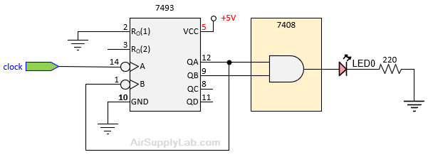
Figure 3.4: Test Circuit
Connect QB and QA to two inputs of a 7408 AND gate. (Do not forget 5V and ground connections; pins 14 and 7. If you forget, the chip is inactive). Referring to the truth tables in 3.1, X = QB, and Y = QA. Connect the clock A input of the counter (pin 14) to the clock signal. Connect QB, QA, to the input of the AND gate, and the output of the AND gate to a LED and verify that the correct outputs are produced by referring to the truth table as shown in Figure 3.5 (or your answer to Exp #3.1).
The truth table and the corresponding waveforms for an AND gate are shown below:
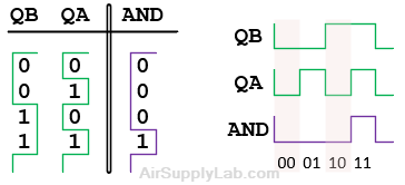
Figure 3.5: The truth table and the corresponding waveforms for an AND gate
Notice that the waveforms are just a graphical form of the truth table (rotated 90 degrees counterclockwise). By displaying such waveforms on a scope, you can obtain a description of circuit behavior equivalent to a truth table.
Actually, you don't need both QB and QA on the scope to know where a complete count cycle starts. It always begins where QB, the MSb (Most Significant bit), falls to 0. Thus, to see how the AND gate output fits into a complete cycle, it only needs to be displayed with QB. (Suppose QA was not shown above. On the scope, you can see that the AND waveform is correctly positioned within a count cycle because it is synchronized with the falling edge of QB.)
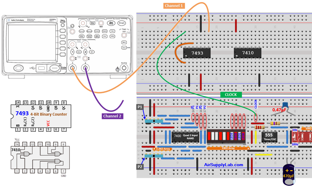
Exp #3.2 Circuit Connection for On-Campus Lab
Connect the clock A input (pin 14 of 7493 Counter) to the timer output (555 Clock output). Switch in the 0.47 μF so the clock frequency will be high (1 kHz). Do this by flipping the capacitor select switch toward the other capacitor (470μF) as you did in a previous experiment. Bring both QB and the AND output to the scope. Adjust the scope's Time/Div until QB goes low for 2 divisions and high for 2 divisions. That way, 4 divisions will represent the full 4-count cycle, QBQA = 00,01,10,11. Thus, QB is 0 (low) for the first two counts and 1 (high) for the next two, exactly as in the above diagram. Then, as the diagram shows, the AND-gate output should remain low for the first 3 counts and go high for the 4th only. (Reminder: instructions on using the scope are found at the end of Lab 02.)
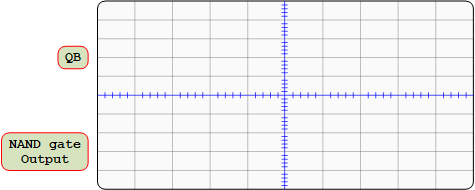
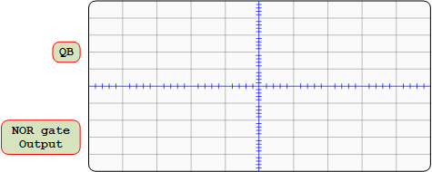
Since a new cycle of 4 counts begins each time QB falls, select a negative edge trigger for the channel that displays QB. (Make sure the trigger level lies within QB's waveform.) Draw the waveforms for QB and the AND output in your lab manual. Repeat for a NAND, OR, XOR, and NOR (do the NOR last since it requires some wiring changes). Leave the scope settings alone as you change gates so QB will look the same in all 5 images.
Connection for 7408 AND
- Attach the first channel of the oscilloscope to QB, and connect the second channel to the output pin of the AND gate.
- Fill in the missing connections on the wiring schematic presented in the figure below


Connection for 7400 NAND
- Attach the first channel of the oscilloscope to QB, and connect the second channel to the output pin of the NAND gate.
- Fill in the missing connections on the wiring schematic presented in the figure below

Connection for 7432 OR
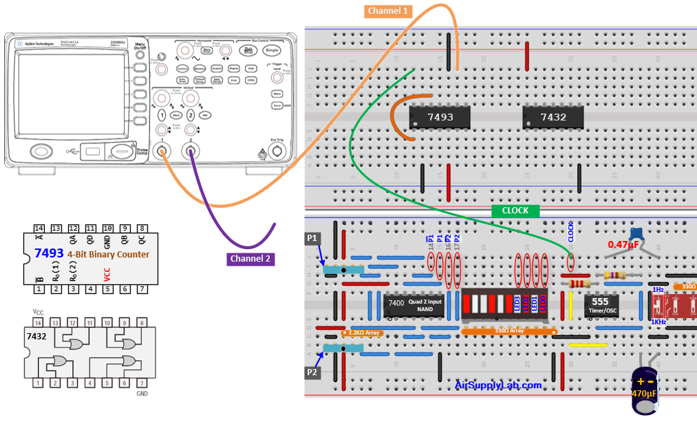
- Attach the first channel of the oscilloscope to QB, and connect the second channel to the output pin of the OR gate.
- Fill in the missing connections on the wiring schematic presented in the figure below

Connection for 7486 XOR
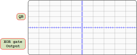
- Attach the first channel of the oscilloscope to QB, and connect the second channel to the output pin of the XOR gate.
- Fill in the missing connections on the wiring schematic presented in the figure below

Connection for 7402 NOR
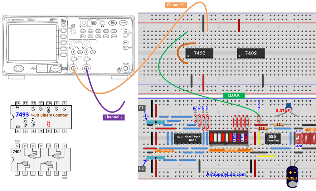
- Attach the first channel of the oscilloscope to QB, and connect the second channel to the output pin of the NOR gate.
- Fill in the missing connections on the wiring schematic presented in the figure below
Question
- For each logic function, draw the wiring diagram of the logic gate (include the pin numbers) in your lab report. You can print out the above wiring diagrams, hand draw the connections, and then scan them into your report. (Totally you must draw 5 wiring diagrams)
- Since a new cycle of 4 counts begins each time QB falls, select a negative edge trigger for the channel that displays QB. (Make sure the trigger level lies within QB's waveform.) Screenshot the oscilloscope waveforms for QB and the AND output in your lab report. Repeat for a NAND, OR, XOR, and NOR (do the NOR last since it requires some wiring changes). Leave the scope settings alone as you change gates so QB will look the same in all 5 images. (Notice: Unplug the +5V wire every time when you are rewiring the connections.)
Diagrams for gate chips are shown below. Note that all have the same power and ground pin numbers (14 and 7). Also, except for the 7402 (NORs), they have exactly the same input and output pin numbers. So, except for the 7402, no wiring changes will be needed as you replace one gate chip with the next. (Remember to remove chips gently so as not to bend pins, and unplug the +5V power wire .)
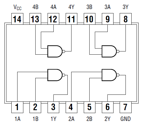
Figure 3.9.1: 7400 Quad NAND Pin Assignment
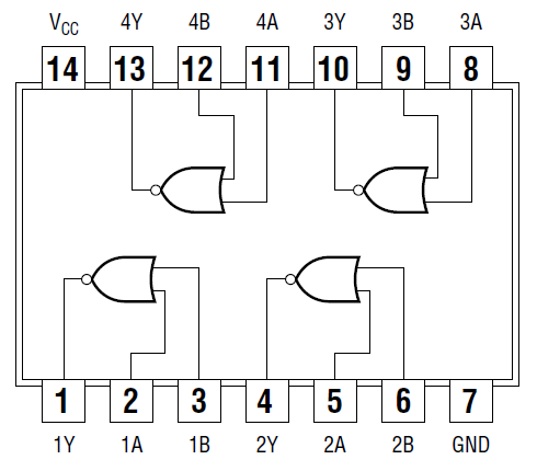
Figure 3.9.2: 7402 Quad NOR Pin Assignment
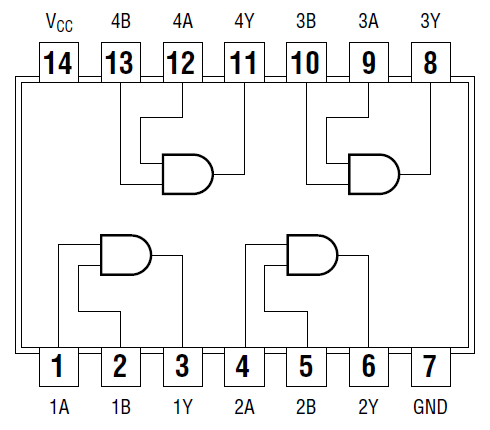
Figure 3.9.3: 7408 Quad AND Pin Assignment
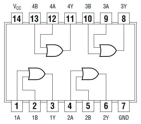
Figure 3.9.4: 7432 Quad OR Pin Assignment
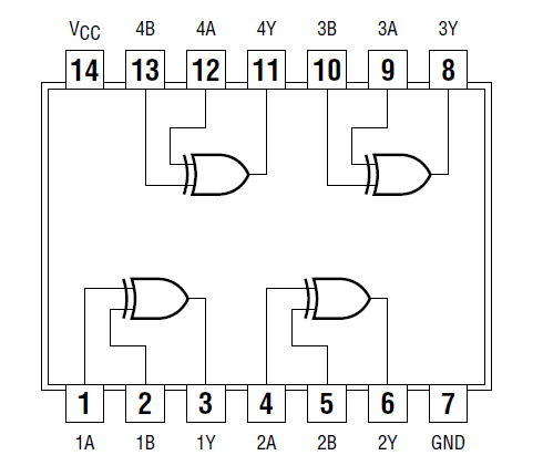
Figure 3.9.5: 7486 Quad XOR Pin Assignment
Exp #3.3 * Test NOT Gate and Three-Input NAND Gate
Repeat the above for a NOT gate and a 3-input NAND gate. For each chip, connect the Q outputs from the counter to drive the logic gates: QA for the NOT gate and QC, QB, QA for the 3-input NAND. The diagrams for the 7404 chip with six ("hex") inverters and the 7410 chip with 3-input NAND gates are shown below. Don't forget to connect power and ground.
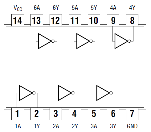
Figure 3.10.1: 7404 Hex Inverter
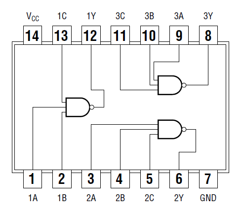
Figure 3.10.2: 7410 Triple 3-Input NAND Gate
The schematics for the NOT and NAND gates are shown below. Connect the inputs of the gates with the appropriate Q output from the counter, i.e., QA for the inverter and QC, QB, QA for the NAND gate.
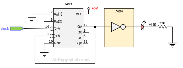
Figure 3.11.1: Schematic for 7404 NOT Gate.
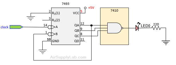
Figure 3.11.2: Schematic for 7410 3-Input NAND Gate.
Question
- For each gate, draw the wiring diagram in your lab report.
- Connect the Oscilloscope/ADALM1000 device to the circuit, and verify the output of the gates that they match your truth table values from Exp #3.1. Screenshot the oscilloscope waveforms and paste them into your report.
- For the 7404 NOT gate, connect QA to AIN (channel 1) , and the output of the NOT gate to BIN (channel 2) of the Oscilloscope/ADALM1000 device.
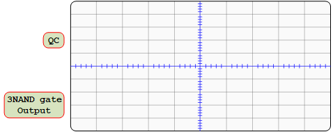
- For the 7410 NAND gate, connect QC (the MSb, most significant input bit) to AIN (channel 1), and the output of the NAND gate to BIN (channel 2) of the Oscilloscope/ADALM1000 device.
Note: since the 7410 NAND has 3 inputs, the counter goes through 8 counts (000 through 111 and back). So, the QC will be low for 4 counts and high for 4 counts before it repeats.
Exp #3.3 Circuit Connection for On-Campus Lab
Connection for 7404 NOT
- Attach the first channel of the oscilloscope to QA, and connect the second channel to the output pin of the NOT gate.
- Fill in the missing connections on the wiring schematic presented in the figure below
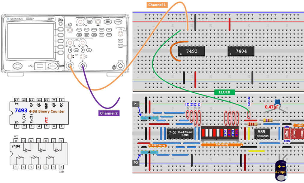

Connection for 7410 NAND
- Attach the first channel of the oscilloscope to QC, and connect the second channel to the output pin of the NAND gate.
- Fill in the missing connections on the wiring schematic presented in the figure below
