Lab 07: Multiplexers and Decoders
Objective
- Design and implement combinational circuits using decoders and multiplexers.
- Learn to simplify designs using a decoder instead of multiple gates.
- Use a multiplexer to implement Boolean functions.
- Analyze and test the circuit designs using an oscilloscope.
- Apply Karnaugh maps to derive and implement logic functions using both decoders and multiplexers.
Required Reading Materials
- Textbook: Digital Design: with an introduction to the Verilog HDL, 5th edition, Mano and Ciletti, ISBN-13: 978-0-13-277420-8
Chapters 3 and 4 - Datasheet: 7410, 7493, 74151, 7155
Components Required
| Component/Device | Description | Quantity |
|---|---|---|
| 7410 Triple 3-Input NAND | × 1 | |
| 7493 4-bit Ripple Counter | × 1 | |
| 74151 8x1 MUX | × 1 | |
| 74155 Dual 2-to-4 Decoder | × 1 |
This experiment deals with alternative ways to build a combinational circuit (one without storage elements, i.e., no flipflops or registers).
In Exp #7.1, your design (which you will build and test) uses a decoder and a couple of gates. This is a much simpler design approach because most of the gates involved are built into the decoder.
In Exp #7.2, your design (again, to be built and tested) is based on a multiplexer (MUX). No external gates are required, so this is probably the simplest design in the experiment.
Experiments
Every experiment section that requires you to build a circuit and test it has an asterisk (*). For those sections:
- For the on-campus lab: Demonstrate the working circuit to your lab instructor.
- For at-home lab: Post pictures of your circuits in the report.
Exp #7.1 * Design with Decoder
(To learn about the decoders, please read Chapter 4 in the textbook.)
Connect the 74LS155 as a 3x8 decoder. Its characteristics are discussed in EE4480-Lab 02: Integer Division Hardware .
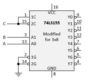
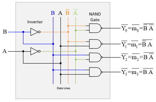
As you can see, the decoder outputs all possible minterms (complemented). So by including a decoder in your circuit, you do not have to use gates to create the minterms you want (as in Lab 6). In this case, you only have to select them at the decoder output and then collect them together with an external OR gate or an invert-OR.
An invert-OR has bubbled inputs that cancel out the bubbles at the decoder outputs. (This cancellation of inverter bubbles was discussed in Lab 6.)
In Lab 6, you started with a map and derived an equation for F by combining squares in the map to simplify the algebra and thereby minimize the amount of hardware (gates) needed for your design. But here, most of the hardware is already inside the decoder, so there's no point in combining map squares and simplifying the algebra to save gates. Trying to do that is a waste of time. As it says above, just collect together the individual minterms you need at the decoder output. Using a decoder makes designing much simpler — almost trivial.
Now, choose functions F1(X,Y,Z) and F2(X,Y,Z) as the following forms:
- F1 should have the form "xxx + xx"; example: X Y Z + Y Z
- F2 should have the form "x + xx"; example: X + Y Z
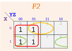
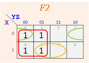
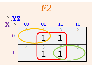
Select the following K maps for your F1 and F2 functions based on your team group number:
In addition to the red circle, select an extraction circle (green, orange, or dark red) for F1 and F2.
Group #1
Group #1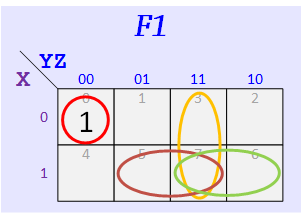
Group #2
Group #2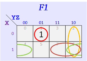
Group #3
Group #3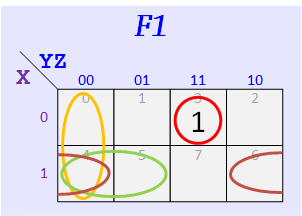
Group #4
Group #4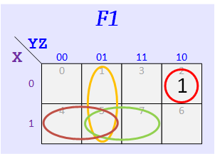
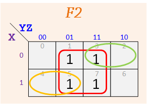
Group #5
Group #5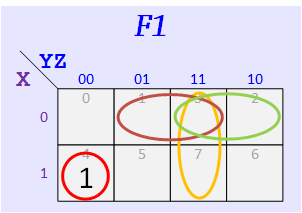
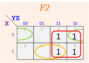
Group #6
Group #6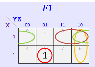
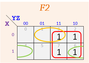
Group #7
Group #7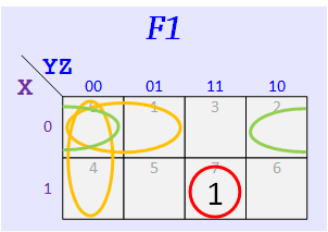
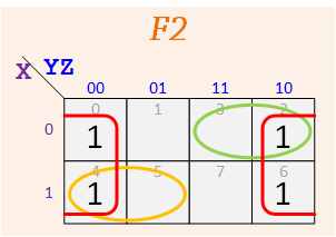
Group #8
Group #8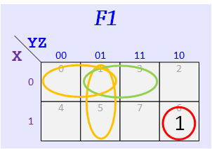
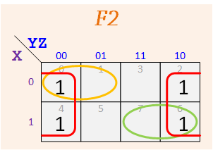
According to the assigned K-Maps, make up your functions — The map for F1 should have three 1's, and the one for F2 should have five.
Express your F1 and F1 as sums of minterms. Example: for F1 given above we get Σ(m0,m4,m7) from the 1's of its map and for F1 we get Σ(m1,m2,m3,m5,m6).
Repeat for F2 and F2.
F1 = Σ m( ), F1 = Σ m( )
F2 = Σ m( ), F2 = Σ m( )
Now, implement the two functions F1(X,Y,Z) and F2(X,Y,Z) using the 74LS155 decoder chip.
- Connect X, Y, and Z to counter outputs QC, QB, and QA.
- Connect X to both pins 1 and 15.
- Connect Y and Z to pins 3 and 13, in that order.
- Connect pins 2 and 14 to the ground. They are active-low enable inputs and must both be low for the decoder to function.

Figure 7.1: The Circuit Diagram for F1 and F2
In addition to the decoder, you will need one 7410 triple 3-input NAND chip (nothing else). F1 should be straightforward. F2 may appear difficult or impossible (since only 3-input gates are available), but it is actually easy (hint: a design for F2 and then do……what?).
Questions
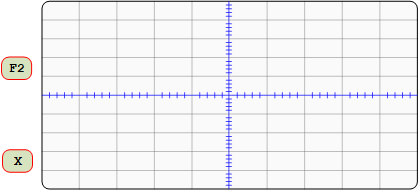
- Testing your design: As in Lab 6, bring X (QC) and F1 to the scope, using a fast clock (1K Hz). Remember to trigger on the falling edge of X, as before. Adjust Time mS/Div on the scope so that one cycle of X spans 8 divisions on the scope screen, one division per count. Then repeat for X and F2. Include scope images in your report, properly labeled. (Copy screen image to flash drive or use camera.)
Make sure your maps agree with the scope images. If they do, comment on this in your report. If not, check to see if you made a mistake in mapping your function F1 or F2. If the map is OK, you may have a connection error in your circuit, which needs to be fixed, or this experiment is not complete. (See the Appendix at the end of Lab 4 for what may be an efficient way to troubleshoot your circuit by mapping scope images.)
Exp #7.1 Circuit Connection for On-Campus Lab
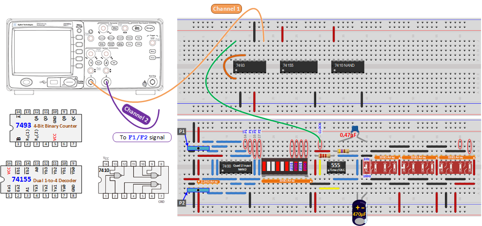
Figure 7.2: The Breadboard Connection for F1 and F2

Exp #7.2 * Design with MUX
Normally, a multiplexer or "MUX" is used as a data-selector; its output is selected from among one or more sets of data inputs. However, MUX can also implement arbitrary boolean functions. They are extensively used for this purpose in programmable chips like FPGAs (field-programmable gate arrays).
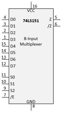
Its data input values, 1's and 0's, are taken from the output column of a function's truth-table. All data inputs equal to 1 are to be connected to power (5V); otherwise, to ground. To find power and ground symbols for your KiCad drawing, click on Component Manager, and open Library Symbols.
For a function F(X,Y,Z), connect X, Y, Z to S2, S1, S0. Each value of XYZ (000...111) selects a data input that is sent to output Z. In a sense, the MUX is like the physical counterpart of a truth-table. The value of XYZ corresponds to a row on the left-hand side of a truth-table, and the right-hand side of that row is the selected value of F. So, in this case, a MUX acts like a Look-Up-Table. To look up the value of F for a given select combination XYZ, you apply that combination to the MUX select inputs, and the answer is supplied at output Z. The term Look-Up-Table is usually shortened to "LUT" in the material dealing with FPGA's.
In FPGA's the LUT's output values can come from an on-chip RAM. By downloading a different set of output values to the RAM while the circuit is in operation, the circuit's function can be completely changed ("on-the-fly" as they say).
Question
-
Use the 74LS151 to implement a function F(X,Y,Z). Choose a function with the form F(X,Y,Z) = xxx + xx + xx, (where x represents an input or its complement) based on your team group number:
In addition to the red circle, select two extraction circles (green, orange, or dark red) for F1.
Group #1
Group #1

Group #2
Group #2

Group #3
Group #3

Group #4
Group #4

Group #5
Group #5

Group #6
Group #6

Group #7
Group #7

Group #8
Group #8

YZ 00 01 11 10 X 0 0
1
3
2
1 4
5
7
6
F(X,Y,Z) =
Proceed as follows:
- Map the function and derive its truth table from the map.
X Y Z F(X,Y,Z) 0 0 0 0 0 1 0 1 0 0 1 1 1 0 0 1 0 1 1 1 0 1 1 1 - Draw the circuit using the KiCad symbol for the 74151. Connect the MUX inputs D0-D7 according to the table (1's connect to 5V, 0's connect to ground). Let X,Y,Z come from counter outputs QC, QB, and QA and connect to them to S2, S1, S0. No need to include the 7493 counter in your diagram; just label inputs as X(QC), Y(QB), and Z(QA)
- Connect the circuit as shown in the diagram. Trigger the counter with a fast clock from the timer output (i.e. change the timer frequency).
Exp #7.2 Circuit Connection for On-Campus Lab
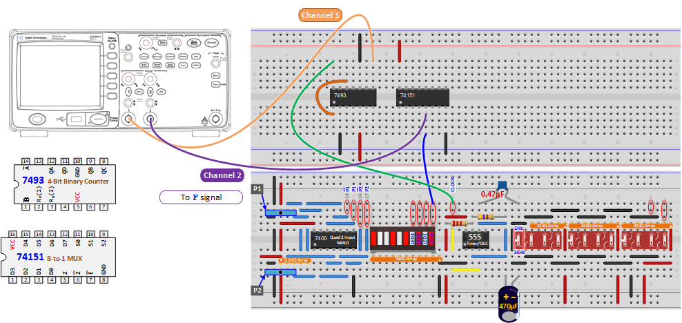
- Verify circuit operation using the oscilloscope. Display F vs. X on the 'scope. Trigger the scope display on the falling edge of X. Show a full cycle of X with a falling edge at the left. Make sure the scope image agrees with your truth-table. If not, fix your connections so it does.
- Map the function and derive its truth table from the map.