FPGA Lab 01: Basic I/O Correspondence between Switch and LED
Software: Intel Quartus Prime Lite v25.1, Questa Starter FPGA Edition 2025.2
Experiment Type: Foundational Verilog FPGA Laboratory
Difficulty: Beginner
Naming Convention: Top-level modules end with _top; testbench modules end with _tb
Important Note:
This experiment requires students to implement the same function twice using two different Verilog modeling methods:
- Gate-level (structural) modeling
- Dataflow modeling
Students must test both versions and compare the two approaches.
The instructor will guide students through the design process in class. A complete final solution is not provided here. After finishing the experiment, students must submit all correct answers, design files, simulation results, and written responses to the instructor
1. Experiment Objective
The objective of this experiment is to understand how physical inputs and outputs on the DE10-Lite board are connected to the FPGA and controlled by a Verilog design. Students will begin with direct switch-to-LED correspondence, then explore alternate logical mapping, and finally design a more advanced LED pattern controller that uses switches to select different visual patterns.
2. Learning Outcomes
- Understand how board-level user I/O devices connect to the FPGA chip
- Create a synthesizable top-level Verilog design using switch and LED ports
- Use Quartus Prime Lite to compile and program the FPGA
- Use Questa Starter FPGA Edition to perform functional simulation
- Distinguish between combinational logic and sequential logic in FPGA design
- Interpret signal mapping, indexing, and visible hardware behavior correctly
- Develop disciplined engineering habits: naming consistency, simulation-first workflow, and hardware verification
3. Pre-Experiment Hardware Background
Before students write any Verilog code, they must understand that the switches and LEDs on the DE10-Lite board are not automatically connected to each other. Both devices are connected to the MAX 10 FPGA, and the FPGA must be programmed to determine how the input signals are interpreted and how the output signals are driven.
3.1 FPGA-Centered Board Architecture
The DE10-Lite board includes 10 LEDs, 10 slide switches, 2 debounced push buttons, and six 7-segment displays. The board block diagram shows that, for user flexibility, the board connections are made via the MAX 10 FPGA. This means the FPGA becomes the central digital system that reads user inputs and drives user outputs.
In practical terms, the signal path in this lab is:
3.2 How the Slide Switches Connect to the FPGA
The DE10-Lite board provides ten slide switches. These switches are used as level-sensitive digital inputs. Each switch is connected directly and individually to a MAX 10 FPGA pin. When a switch is in the DOWN position, closest to the edge of the board, it provides a logic 0 to the FPGA. When the switch is in the UP position, it provides logic 1 to the FPGA.

Therefore, for this experiment:
- A slide switch behaves like a stable logic input, not a short pulse
- No clock is required to read the switch value
- No debouncing logic is needed for the slide switches in this lab
- Each switch must be interpreted through the FPGA design
3.3 How the Red LEDs Connect to the FPGA
The board also provides ten user-controllable red LEDs. Each LED is driven directly and individually by a MAX 10 FPGA pin. Driving the corresponding FPGA pin to logic high turns the LED on, and driving the pin to logic low turns the LED off. Therefore, the DE10-Lite red LEDs behave as active-high outputs.

Therefore, for this experiment:
- An LED can be treated as a standard digital output
- Logic 1 turns the LED on
- Logic 0 turns the LED off
- Each LED is independently driven by the FPGA design
3.4 Signal Names Used in This Lab
The user I/O signal names used in this lab are:
- SW[9:0] for the ten slide switches
- LEDR[9:0] for the ten red LEDs
Students must ensure that the Verilog port names match the project pin assignments exactly.
3.5 Notes About Other Board Resources
- KEY[1:0]: Push buttons are active-low and already include board-level debouncing
- All 7-segment displays are active-low
- These resources are not required in Experiment 1A, but students should remember their logic conventions for future labs
3.6 Why This Matters Before Coding
This first experiment is not just about making LEDs light up. It is about learning the engineering chain that connects physical hardware, HDL, synthesis, simulation, and board-level verification. Students should understand that even a very simple design requires correct module naming, port declarations, pin mapping, bit ordering, and verification steps.
4. Pre-Lab Thinking Questions
- Why do the switches not control the LEDs automatically, even though both are on the same board?
- What does it mean that a switch is connected directly to an FPGA pin?
- Why is a slide switch considered level-sensitive?
- Why is an LED considered an output device from the FPGA point of view?
- What can go wrong if the Verilog port names do not match the Quartus pin assignments?
- If the LEDs were active-low instead of active-high, what would change in the design?
5. General Lab Rules
- Use the DE10-Lite board only; no external hardware is required
- Use the provided Quartus Setting File as the pin-assignment reference
- Simulate the design before programming the FPGA board
- Use consistent naming and project organization
- Do not submit copied work; all answers and source files must reflect your own understanding
Experiment 1A: Direct Switch-to-LED Correspondence
Experiment 1A: Direct Switch-to-LED Correspondence
Learn how to connect the ten slide switches directly to the ten red LEDs using a simple synthesizable combinational design.
A top-level Verilog design in which each switch directly controls the corresponding LED. This is the most basic FPGA input/output mapping experiment and serves as the foundation for future labs.
- Project name:switch_to_led
- Top-level module: switch_to_led_top
- Testbench module: switch_to_led_tb
- Inputs: SW[9:0]
- Outputs: LEDR[9:0]
- LEDR[0] must reflect SW[0]
- LEDR[1] must reflect SW[1]
- ...
- LEDR[9] must reflect SW[9]
- No clock is required
- No reset is required
- The design must be purely combinational
- Declare a 10-bit input vector for switches and a 10-bit output vector for LEDs
- Keep the design simple and synthesizable
- Verify width consistency carefully
- Confirm the top-level module name is set correctly in Quartus
module switch_to_led_top (
    input  [9:0] SW,
    output [9:0] LEDR
);

// Student implementation goes here

endmodulemodule switch_to_led_tb;
// Testbench signals go here
// Instantiate switch_to_led_top
// Apply test patterns
endmodule- Instantiate switch_to_led_top
- Apply multiple patterns to SW[9:0]
- Observe whether LEDR[9:0] matches the switch pattern correctly
- Test at least:
- all zeros
- all ones
- alternating patterns
- one-hot patterns
- Why is this design combinational rather than sequential?
- Why is no
always @(posedge clk)block needed? - Why is simulation still necessary for such a simple design?
- What kind of mistake would cause the wrong LED to respond in hardware?
- Why must the top-level ports correspond to real FPGA board signals?
Experiment 1B: Alternate LED Mapping
Experiment 1B: Alternate LED Mapping
Understand that the same physical I/O resources can produce different logical behaviors depending on how the signals are mapped in Verilog.
A modified switch-to-LED design in which the logical correspondence is intentionally changed. One recommended version is a reversed mapping: the lowest-numbered switch controls the highest-numbered LED, and the highest-numbered switch controls the lowest-numbered LED.
- Top-level module:
switch_to_led_reverse_top - Testbench module:
switch_to_led_reverse_tb
SW[0]controlsLEDR[9]SW[1]controlsLEDR[8]- ...
SW[9]controlsLEDR[0]
- Do not change the board pin assignments
- Only change the logical mapping in the Verilog design
- Document the new relationship clearly
- Use simulation to confirm the revised behavior before board testing
- Is the reverse-mapping design still combinational? Explain.
- Which part changed: the board hardware, the Quartus pin assignment, or the Verilog logic?
- How can a simple indexing error cause a hardware mismatch?
- Why is clear mapping documentation important in engineering work?
- If the original design works but the modified one behaves incorrectly, what should be checked first?
Experiment 1C: LED Pattern Controller with Pattern Selection
Experiment 1C: LED Pattern Controller with Pattern Selection
Extend the lab topic into a more advanced design that introduces timing, sequencing, visible animation, and pattern selection using switches.
A small LED pattern controller that generates multiple visible LED patterns similar to police or emergency lighting. Switches are used to select the active pattern, and the FPGA clock is used to update the pattern at a human-visible speed.
- Top-level module:
switch_to_led_pattern_top - Testbench module:
switch_to_led_pattern_tb
- Inputs:
CLOCK_50, selected bits ofSWfor pattern selection - Outputs:
LEDR[9:0]
- Pattern 0: Turn on LEDs one by one from
LEDR[0]toLEDR[9], then fromLEDR[9]back toLEDR[0] - Pattern 1: Blink
LEDR[4:0], then blinkLEDR[9:5], repeating continuously - Pattern 2: Alternate the lower half and upper half of the LED array
- Pattern 3: A student-designed custom pattern
SW[1:0]: pattern selectSW[2]: optional speed selection- Remaining switches: reserved or optional extension
- Use
CLOCK_50as the timing source - Make the visible update rate slow enough for human observation
- Use switches to select or modify the pattern
- Keep the design synthesizable
- Simulate the design before downloading to the FPGA board
- Do not treat this as a purely combinational design
- A visible LED pattern requires timing and state progression
- Use a counter-based timing method to slow down pattern updates
- Prefer a clock-enable pulse approach for pattern updates rather than creating unnecessary internal fabric clocks
- Separate timing logic from pattern-generation logic as much as possible
- Why can a running LED pattern not be implemented as pure combinational logic?
- Why is a timing mechanism required for visible LED animation?
- What is the difference between a divided clock and a clock-enable pulse?
- How would you organize the design if more patterns were added later?
- What should be adjusted if the pattern speed is too fast to observe?
- Why is it useful to separate timing, control, and output logic into different parts of the design?
9. Recommended Design Workflow
- Create the Quartus project and select the correct MAX 10 device
- Set the correct top-level entity name
- Add the Verilog source file(s)
- Use the provided QSF reference for pin assignment consistency
- Compile the design and fix all syntax or naming errors
- Create the correct testbench module
- Run functional simulation in Questa Starter FPGA Edition 2025.2
- Verify the waveform behavior carefully
- Program the DE10-Lite board
- Compare hardware behavior with the expected design behavior
10. Common Mistakes to Avoid
- Wrong top-level module name
- Wrong testbench module name
- Signal names that do not match the intended board resource names
- Incorrect bit width or vector indexing
- Skipping simulation
- Programming the board before the compile is clean
- Using a clock in Experiment 1A when none is needed
- Trying to implement visible LED animation in Experiment 1C without timing logic
11. Deliverables
Students must submit all correct files and all written answers to the instructor.
- All correct Verilog source files for the completed sub-experiments
- All correct testbench files
- Simulation waveform screenshots
- Hardware verification photo(s) or screenshot(s)
- Complete written answers to all pre-lab and post-lab questions
- A short reflection on what was learned, what errors occurred, and how they were resolved
12. Final Reflection Questions
- What is the most important thing you learned from this lab about FPGA hardware interaction?
- What was the difference between a logical design error and a project setup error?
- Why is this first experiment important even though the initial design is simple?
- How does this lab prepare you for later labs involving counters, FSMs, displays, and more advanced timing behavior?
13. Submission Reminder
- Your project and module names follow the required naming convention
- Your design compiles without errors
- Your simulation results match your design intent
- Your hardware results match your simulation results
- All answers are complete and ready to submit to the instructor
FPGA Lab 01: Switches, LEDs, and Multiplexers
Objective
The purpose of this exercise is to learn how to connect simple input and output devices to an FPGA chip and implement a circuit that uses these devices. We will use the switches on the DE10-Lite board as inputs to the circuit. We will use light-emitting diodes (LEDs) as output devices.
Required Reading Materials
- Textbook: Digital Design: with An Introduction to the Verilog HDL, VHDL, and SystemVerilog, 6th edition, Mano and Ciletti, ISBN-13: 978-0-13-454989-7
Ch 4.5 - Lesson 01: Create a New FPGA Project using Quartus Prime Standard
- Lesson KB 02: Intel DE10-Lite Board
Overview
DE10-Lite FPGA Board Switches and LEDs
The Intel DE10-Lite FPGA board has ten switches and LEDs. The connections between the switches and LEDs are shown in the following Figures:
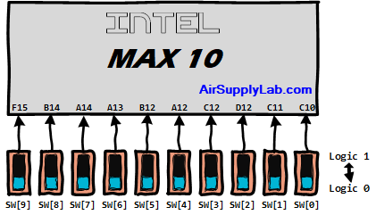
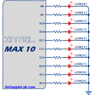
Figure 1: The Connections of Switches and LEDs on the DE10-Lite FPGA Board
Multiplexers (MUX)
In digital circuits, a multiplexer (or MUX) is a device that selects one of several digital input signals and forwards the selected input into a single line. A multiplexer of 2n inputs has n select lines, which are used to select which input line to send to the output.
- A 2n-to-1 multiplexer sends one of the 2n input lines to a single output line.
- A multiplexer has two sets of inputs:
- 2n data input lines
- n select lines to pick one of the 2n data inputs
- The mux output is a single bit, which is one of the 2n data inputs.
2-to-1 1-bit MUX
Figure 2 (b) shows a sum-of-products circuit that implements a 2-to-1 multiplexer with a select input s. If s = 0, the output of the multiplexer (out) is equal to the input in0; if s = 1, the output is equal to in1. Part (a) of the figure gives a function table for this multiplexer, and part (c) shows its circuit symbol.
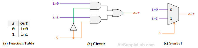
Figure 2: A 2-to-1 Multiplexer
2-to-1 4-bit MUX
Write a Verilog module with four assignment statements like the one shown above to describe the circuit given in Figure 3 (a). This circuit has two four-bit inputs, In0 and In1, and produces the four-bit output Out. If S = 0 then Out = In0, while if S = 1 then Out = In1. We refer to this circuit as a four-bit wide 2-to-1 multiplexer, and its circuit symbol shows in Figure 3(b), in which In0, In1, and Out depict as four-bit wires.
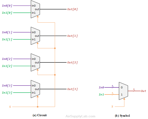
Figure 3: A four-bit wide 2-to-1 Multiplexer
4-to1 1-bit MUX
A 4-to-1 MUX takes four inputs and directs a single selected input to output. A 2-bits selection input controls the selection of input. The characteristic table of 4-to-1 MUX is shown below:
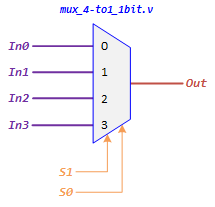
| Select Lines | Output | |
|---|---|---|
| S1 | S0 | Out |
| 0 | 0 | In0 |
| 0 | 1 | In1 |
| 1 | 0 | In2 |
| 1 | 1 | In3 |
Figure 4: A 4-to-1 Multiplexer
The logic Circuit Diagram of 4-to-1 MUX is shown in the following Figure:
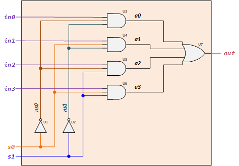
Figure 5: 4-to-1 1-bit MUX Logic Circuit
Lab Experiments
1.1 Connect Switches to LEDR
The DE10-Lite provides ten switches and lights, called SW9-0 and LEDR9-0. The switches can provide input signals, and the lights can be used as output devices. To directly connect each input to the outputs, the buffer gate can be used in this situation. The following diagram shows a simple circuit with ten buffers connecting switches and LEDs.
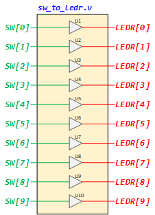
Figure 6: Using Buffers To Connect the SWs to LEDRs
Besides the Gate-Level modeling, we also can use Data Flow modeling to describe the circuit as follow:
assign LEDR[0] = SW[0];
assign LEDR[1] = SW[1];
assign LEDR[2] = SW[2];
assign LEDR[3] = SW[3];
assign LEDR[4] = SW[4];
assign LEDR[5] = SW[5];
assign LEDR[6] = SW[6];
assign LEDR[7] = SW[7];
assign LEDR[8] = SW[8];
assign LEDR[9] = SW[9];
Since there are multiple switches and lights, and they have the same size (bit width), it is convenient to represent them as a vector in the Verilog code, as shown. We have used a single assignment statement for all LEDR outputs, which is equivalent to the individual assignments:
assign LEDR = SW;
Lab Procedures
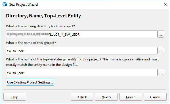
- Launch Altera Quartus Prime and click on File ➤ New Project Wizard to create a new project for your circuit.
- The New Project Wizard dialog will be displayed. Enter the directory and the new name for the project and top-level module name as below:
- Project working directory: <your project home folder>\Lab01.1_SW_LEDR
- Project name: sw_to_ledr
- Top-level module name: sw_to_ledr
- Create a new Verilog HDL file, implement the circuit using gate-level modeling to describe the Figure 6 circuit, and save it to sw_to_ledr.v file.
module sw_to_ledr(SW, LEDR); input [9:0] SW; // Slide Switches output [9:0] LEDR; // Red LEDs // Using Gate-Level modeling to connect SWs to LEDRs endmodule - Compile the project by clicking Processing ➤ Start Analysis & Elaboration.
- Open the RTL Viewer to check the connections by clicking the Tools ➤ Netlist Viewers ➤ RTL Viewer.
- If any connection is incorrect, fix it in the sw_to_ledr.v, and redo step 4.
- Import the pin assignment file to your project.
- Compile the project by clicking Processing ➤ Start Compilation.
- Download the compiled object file to the FPGA board using the Quartus Programmer tool.
- Test the circuit's functionality by toggling the switches and observing the LEDs.
Question
- Set the switch to the values shown below (logic-0 means slide down and logic-1 slides up) to see the result on the LEDs. Take pictures of each iteration.
- SW[9:0] = 1111 0000
- SW[9:0] = 0000 1111
- SW[9:0] = 1100 1100
- SW[9:0] = 0101 0101
1.2 Four-bit Wide 2-to-1 Multiplexer
Design a four-bit wide 2-to-1 multiplexer as the following figure — Use switch SW[9] as the S input, switches SW[3:0] as the In0 input, and SW[7:4] as the In1 input. Display the value of the input S on LEDR[9], connect the output Out to LEDR[3:0], and connect the unused LEDR lights to the constant value 0.
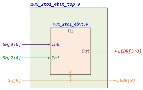
Figure 7: Top Module of a Four-Bit Width 2-to-1 Multiplexer
Lab Procedures
- Create a new Quartus project for your circuit by entering the following information:
- Project working directory: <your Project home folder>\Lab01.2_Multiplexer
- Project name: mux_2to1_4bit
- Top-level module name: mux_2to1_4bit_top
- Create a new Verilog HDL file to implement the top-level module. Type the following Verilog and complete the connections based on Figure 7, then save it to mux_2to1_4bit_top.v
module mux_2to1_4bit_top(SW, LEDR); input [9:0] SW; output [9:0] LEDR; mux_2to1_4bit U1 (.In0(__), .In1(__), .S(__), .Out(__)); // Connect LEDR[9] to SW[9] assign _______; endmodule - Create a new Verilog HDL file to implement the 2-to-1 1-bit MUX by using Gate-level modeling to describe the circuit, as shown in Figure 2(b). Save the file to mux_2to1_1bit.v
module mux_2to1_1bit(in0, in1, s, out); input in0, in1, s; output out; // Using Gate-Level Modeling to desctibe the 2-to-1 1bit MUX circuit here endmodule - Create a new Verilog HDL file to implement the 2-to-1 1-bit MUX by using Gate-level modeling to describe the circuit, as shown in Figure 3(a). Save the file to mux_2to1_4bit.v
module mux_2to1_4bit(In0, In1, S, Out); input [3:0] In0; input [3:0] In1; input S; output [3:0] Out; // Connect four 2-to-1 1bit MUX mux_2to1_1bit U1 (.in0( ), .in1( ), .s( ), .out( ) ); mux_2to1_1bit U2 (.in0( ), .in1( ), .s( ), .out( ) ); mux_2to1_1bit U3 (.in0( ), .in1( ), .s( ), .out( ) ); mux_2to1_1bit U4 (.in0( ), .in1( ), .s( ), .out( ) ); endmodule - Click [Start Analysis & Elaboration] to compile your design. Make sure there are no syntax errors.
- After you perform a successful Analysis & Elaboration, you can view the design in the RTL Viewer by clicking Tools ➤ Netlist Viewers ➤ RTL Viewer. Screenshot the RTL diagrams for top, 2-to-1 4bit, and 2-to1 1bit modules.
- Import pin assignments to the project.
- Fully compile the project by clicking Processing ➤ Start Compilation. After success compelling, program the object file (mux_2to1_4bit_top.sof) to the FPGA board.
- Test the functionality of the four-bit wide 2-to-1 multiplexer by toggling the switches and observing the LEDs.
Question
- Post your RTL diagrams for the top-level module, 2-to-1 4-bit module, and 2-to-1 1-bit module in your report.
- Test your design and fill in the results in the following table.
SW[9] SW[7:4] SW[3:0] LEDR[9] LEDR[3:0] 0 0101 1111 1 0101 1111 0 1100 1001 1 1100 1001 0 0011 0110 1 0011 0110
1.3 Implement 8-to-1 Multiplexer
In this experiment, you will design an 8-to-1 MUX using two 4-to-1 MUX and one 2-to-1 MUX.
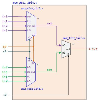
Figure 8: Build an 8-to-1 1-bit MUX using Two 4-to-1 and One 2-to-1 MUXs
Lab Procedures
- Launch Altera Quartus Prime and click on File ➤ New Project Wizard to create a new project for your circuit.
- The New Project Wizard dialog will be displayed. Enter the directory and the new name for the project and top-level module name as below:
- Project working directory: <your project home folder>\Lab01.3_MUX_8TO1
- Project name: mux_8to1_1bit
- Top-level module name: mux_8to1_1bit
- Add the mux_2to1_1bit.v file from the Lab01_2_Multiplexer folder into the project.
- Create a new Verilog HDL file to implement the top-level module. Type the following Verilog and complete the connections based on Figure 8, then save it to mux_8to1_1bit.v.
module mux_8to1_1bit(in0, in1, in2, in3, in4, in5, in6, in7, s0, s1, s2, out); input in0, in1, in2, in3, in4, in5, in6, in7; // Input Pins input s0, s1, s2; // Selection Pins output out; // Output Pin wire out0, out1; // Using Structural (Gate-Level) modeling to implement 8-to-1 MUX mux_4to1_1bit U1 (.in0(), .in1(), .in2(), .in3(), .s0(), .s1(), .out()); mux_4to1_1bit U2 (.in0(), .in1(), .in2(), .in3(), .s0(), .s1(), .out()); mux_2to1_1bit U3 (.in0(), .in1(), .s(), .out()); endmodule - Create a new Verilog HDL file to implement the 4-to-1 1-bit MUX using Gate-level modeling to describe the circuit, as shown in Figure 6. Save the file to mux_4to1_1bit.v.
module mux_4to1_1bit(in0, in1, in2, in3, s0, s1, out); input in0, in1, in2, in3; // Input Pins input s0, s1; // Selection Pins output out; // Output Pin wire ns0, ns1, a0, a1, a2, a3; // Using Gate-Level modeling to implement 4-to-1 MUX endmodule - Create a new Verilog HDL file to implement a testbench file. Copy the following code and save it to mux_8to1_1bit_tb.v.
`timescale 1ns/1ps module mux_8to1_1bit_tb(); reg in0, in1, in2, in3, in4, in5, in6, in7; reg s0, s1, s2; wire out; mux_8to1_1bit DUT(.in0(in0), .in1(in1), .in2(in2), .in3(in3), .in4(in4), .in5(in5), .in6(in6), .in7(in7), .s0(s0), .s1(s1), .s2(s2), .out(out)); initial begin in0 = 1'b0; in1 = 1'b1; in2 = 1'b1; in3 = 1'b1; in4 = 1'b0; in5 = 1'b0; in6 = 1'b1; in7 = 1'b1; s0 = 1'b0; s1 = 1'b0; s2 = 1'b0; #1 $display("s2=%d s1=%d s0=%d out=%d \n", s2, s1, s0, out); #5 s0 = 1'b0; s1 = 1'b0; s2 = 1'b1; #1 $display("s2=%d s1=%d s0=%d out=%d \n", s2, s1, s0, out); #5 s0 = 1'b0; s1 = 1'b1; s2 = 1'b0; #1 $display("s2=%d s1=%d s0=%d out=%d \n", s2, s1, s0, out); #5 s0 = 1'b0; s1 = 1'b1; s2 = 1'b1; #1 $display("s2=%d s1=%d s0=%d out=%d \n", s2, s1, s0, out); #5 s0 = 1'b1; s1 = 1'b0; s2 = 1'b0; #1 $display("s2=%d s1=%d s0=%d out=%d \n", s2, s1, s0, out); #5 s0 = 1'b1; s1 = 1'b0; s2 = 1'b1; #1 $display("s2=%d s1=%d s0=%d out=%d \n", s2, s1, s0, out); #5 s0 = 1'b1; s1 = 1'b1; s2 = 1'b0; #1 $display("s2=%d s1=%d s0=%d out=%d \n", s2, s1, s0, out); #5 s0 = 1'b1; s1 = 1'b1; s2 = 1'b1; #1 $display("s2=%d s1=%d s0=%d out=%d \n", s2, s1, s0, out); #5 $stop; end endmodule - Click Start Analysis & Elaboration to compile your design. Make sure there are no syntax errors.
After you perform a successful Analysis & Elaboration, you can view the design in the RTL Viewer by clicking Tools ➤ Netlist Viewers ➤ RTL Viewer. Screenshot the RTL diagrams for mux_8to1_1bit, and mux_4to1_1bit modules. - If there are no errors, click RTL Simulation to simulate and test the 8-to-1 MUX.
- Screenshit the waveform.