Lab 10: Introduction to Sequential Logic
Objectives
- Understand the basics of sequential logic circuits and how they differ from combinational logic.
- Learn the function of flip-flops (SR, JK, D, and T flip-flops) in holding state information.
- Explore the behavior of D and JK flip-flop circuits.
- Experiment with building T flip-flops from JK flip-flops.
- Design and implement circuits to demonstrate the working of D and T flip-flops.
Required Reading Materials
- Textbook: Digital Design: with an introduction to the Verilog HDL, 5th edition, Mano and Ciletti, ISBN-13: 978-0-13-277420-8
Chapter 5 - Datasheet: 7474, 7476, 7486
Components Required
| Component/Device | Description | Quantity |
|---|---|---|
 |
Breadboard | × 1 |
| 7474 Dual D Flip-Flop | × 1 | |
| 7476 Dual J-K Flip-Flop | × 1 | |
| 7486 Quad 2-Input XOR | × 1 | |
| Digilent Analog Discovery 2 (AD2) or Analog Devices ADALM1000 (M1K) |
× 1 |
Experiments
Every experiment section that requires you to build a circuit and test it has an asterisk (*). For those sections:
- For the in-class lab: Demonstrate the working circuit to your lab instructor.
- For online lab: Take a video to describe your circuit, upload the video to YouTube, and put the link in the report.
Exp #10.1 Sequential Logic Circuits
Sequential logic circuits are a type of logic circuit where the output of the circuit depends not only on the input, as in combinational logic circuits, but also on the sequence of past inputs that determine the present state of the circuit. For example, consider an elevator controller in a five-story building: if someone on the third floor pushes the down button, should the elevator controller tell the elevator to go up or down to pick up the passenger on the third floor? You cannot answer that question without knowing what floor the elevator is currently on. If it is on the 4th or 5th floor, the elevator must go down to the 3rd floor. If it is on the 1st or 2nd floor, it must go up to the 3rd floor. And if it is already on the 3rd floor it doesn't need to go up or down. The current floor of the elevator is one of the variables that would be used to determine the state of the elevator. There can be other state variables as well for the elevator control system. For example, there may be a state variable to indicate whether the elevator is currently moving up, currently moving down, or stationary.
Flip-flops are memory devices used to hold the state in a sequential logic circuit. A flip-flop can hold 1-bit of a state variable (i.e. one binary value). The output of a flip-flop, typically named Q, represents the state of the flip-flop. Usually, the complement of the state, Q, is also available at the output. There are three types of inputs for flip-flops, the clock input, the synchronous input, and the asynchronous inputs.
- The clock input is used to control when the state should change or transition. We say that the clock triggers the state change (transition). There are different mechanisms for triggering a flip-flop. The most common is to trigger a flip-flop on either the rising (positive) edge of the clock ↑ or on its falling (negative) edge ↓. The following figures show the two types of triggers. Note that the triangle symbol (>) is used to show that it is an edge-triggered flip-flop and the bubble in front of the triangle indicates that it is a negative edge-triggered flip-flop.
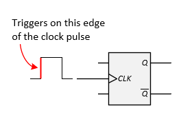
Positive Edge Triggering
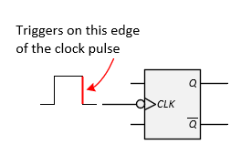
Negative Edge Triggering
- The synchronous inputs are used to determine how the flip-flop should change state when it is triggered. ("synchronous" implies that the inputs are synchronized with the clock.) There are four types of flip-flops as shown in the figure below. The figure shows the name of the flip-flop (SR, JK, D, and T), the logic symbol for the flip-flop, the characteristic table of the flip-flop that describes how it behaves ("Q(next)" is the next state of the flip-flop after the trigger), the characteristic equation that captures the behavior in a Boolean expression, and the Excitation table that shows how to control the synchronous inputs to get the desired state transition (from the present state Q to the next state Q(next)). You will see various ways to describe the next state including Q(next), Q(t+1), Qt+1, and Q+. We'll use Q(t+1).
| FLIP-FLOP NAME | FLIP-FLOP SYMBOL | CHARACTERISTIC TABLE | CHARACTERISTIC EQUATION | EXCITATION TABLE | |||||||||||||||||||||||||||||||||||
|---|---|---|---|---|---|---|---|---|---|---|---|---|---|---|---|---|---|---|---|---|---|---|---|---|---|---|---|---|---|---|---|---|---|---|---|---|---|---|---|
| SR | 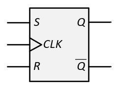 |
|
Q(next) = S + R Q S R = 0 |
|
|||||||||||||||||||||||||||||||||||
| JK | 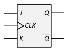 |
|
Q(next) = J Q + K Q |
|
|||||||||||||||||||||||||||||||||||
| D | 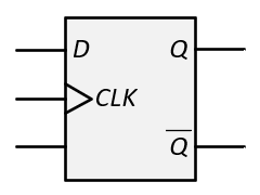 |
|
Q(next) = D |
|
|||||||||||||||||||||||||||||||||||
| T | 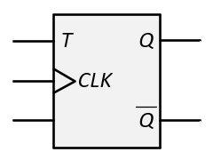 |
|
Q(next) = T Q + T Q |
|
Let's look at the four types of flip-flops in more detail (note: changes in Q occur only at the triggering edge of the clock).
-
- SR Flip-flop
This is a set-reset flip-flop. When S = 1, R = 0, the flip-flop is set, Q(t+1) = 1. When R = 1, S = 0, the flip-flop is reset, Q(t+1) = 0. When both S and R are 0, there is no change, Q(t+1) = Q(t). The SR flip-flop has undefined behavior when both S and R are 1. For this reason, SR flip-flops are not often used. - JK Flip-flop
A JK flip-flop is similar to an SR flip-flop, where setting J = 1, K = 0, will set the flip-flop, K = 1, J = 0, will reset the flip-flop, and having both J and K equal to 0 will result in no change. The JK flip-flop differs from the SR since when both inputs are 1, the state will toggle (be complemented), that is, Q(t+1) = Q(t). - D Flip-flop
This flip-flop is known as a data flip-flop. The state of the D flip-flop will follow the D input. When the flip-flop is clocked, if D = 0, Q(t+1) will be 0 and if D = 1, Q(t+1) will be 1. Thus, the D flip-flop behaves like a memory element, remembering the value on the D input in the state Q; i.e. Q(t+1) = D. - T Flip-flop
This is a toggle flip-flop. When T = 0, the state will be unchanged, Q(t+1) = Q(t), and when T = 1, the state will toggle (be complemented), that is Q(t+1) = Q(t).
- SR Flip-flop
- The third type of inputs are asynchronous inputs. Whereas synchronous inputs only effect the state of the flip-flop on the positive or negative edge of the clock (depending on the type of flip-flop), asynchronous inputs override the synchronous inputs (take priority over them) and also do not depend on the clock.
When an asynchronous input is active, it will immediately effect the state of the flip-flop (it does not wait for the clock). Flip-flops usually have two asynchronous inputs, preset (PR) and clear (CLR). PR is used to set the state (set Q to 1); CLR is used to clear the state (clear Q to 0). The asynchronous inputs are often active-low which means that they will be active when a low voltage is applied to them and inactive when a high voltage is applied. A bubble is often used to indicate that the asynchronous input is active-low; alternatively, there may be a bar over its name or a slash / in front (like /CLR) to indicate that it is active-low.
The asynchronous inputs are used to initialize flip-flops to a known state on power-up or to reset a state to a known value during normal operation. When the asynchronous inputs are inactive, the flipflop will be controlled by the clock and synchronous inputs. Note, you should not have both preset and clear inputs active at the same time as the effect on the state will be unpredictable.
Exp #10.2 * Exploring the behavior of a D Flip-flop
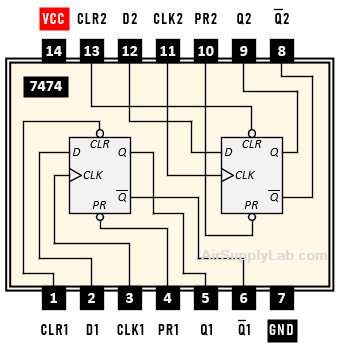
Below is the diagram for a 7474 dual D Flip-flop chip.
Questions
- Answer the following questions in your report.
- Are the flip-flops positive-edge triggered or negative-edge triggered? Explain how you know.
- Are the preset (PR) and clear (CLR) asynchronous inputs active-high or active-low? Explain how you know.
- Since there are two flip-flops, how many states can be represented using one 7474?
Consider the fact that there are two state variables (Q1 and Q2). To help you figure out the answer, complete the following table below and include it in your lab notebook.
Indicate the total number of possible states that can be represented using Q1 and Q2.
Table 1: For Question 1.c
| Q1 | Q2 | States |
|---|---|---|
| 0 | 0 | 0 (00) |
| 0 | 1 | 1 (01) |
| 1 | 0 | |
| 1 | 1 |
Referring to the 7474 pin assignments above, draw a wiring diagram to test the behavior of a D flip-flop.
- Hand draw the logic diagram of one of the D flip-flops (not the entire chip) and label all of the pin numbers for the inputs and outputs accordingly.
- Include this power and ground table in your Circuit Diagram.
Unit Chip Power Pin Ground Pin 1 7474 14 7 - In the diagram, connect the PR and CLR inputs to toggle switches and set both inactive (you need to determine if connecting to power (high) or to the ground (low) will make them inactive).
- Connect the clock input (CLK) to the pushbutton switch (pulser). Although the 7474 triggers on the clock's positive edge, you can use either pulser output (normally high or low) since either way the clock pulse has a positive edge:
or
.
If you use the ADALM1000 device, you have to connect to PIO 0. Check Lab 02 Exp#2.2 to learn how to use the PIO function.
You may prefer to use KiCad. You won't have to label pin numbers since all chip numbers and pin numbers including Vcc and Ground are already included in the diagram. Therefore, a power and ground table is not needed. For the clock, instead of a pushbutton switch symbol, just use a "port" symbol from the Library Symbol listing:
In the wiring diagram, connect the D input to one of the toggle switches and connect the Q output to one of the LEDs and Q to another LED. With KiCad just use port symbols
.
After you complete the wiring diagram, wire the circuit as shown in your diagram using the 7474 chip, a clock (CLK), three toggle switch (D, PR, CLR), and two LEDs (Q and Q). Test your circuit following the characteristic table shown below.
- In the first 3 lines, to make PR or CLR high or low, connect them to power or ground through the switches. Observe the outputs on the LEDs and insert them into the Next State columns. The X's indicate that changes in CK and D should have no effect on Q(t+1). Show that this is true for each of the first 3 lines of the table by toggling D up and down and then by pulsing the clock.
- In the last 2 lines, PR and CLR are connected to power and so are inactive. For each line, toggle the clock after you have set D to the value shown. Then enter the results into the Next State columns.
Table 2: Characteristic Table of D Flip-Flop
| Inputs | Next State | ||||
|---|---|---|---|---|---|
| PR | CLR | CLK | D | Q(t+1) | Q(t+1) |
| Low (0) | High (1) | X | X | ||
| High (1) | Low (0) | X | X | ||
| Low (0) | Low (0) | X | X | ||
| High (1) | High (1) | ↑ | Low (0) | ||
| High (1) | High (1) | ↑ | High (1) | ||
- For the on-campus lab, demonstrate your circuit to your instructor.
- For the online lab, take a video to demonstrate your circuit, and put the YouTube link in your report.
Questions
- Answer the following questions in your report:
- When PR is low, does changing the clock or D input have any effect on Q and Q?
- Repeat when CLR is low.
- How does Q(t+1) correspond to Q(t+1)? Are there any cases when it doesn't behave as expected?
- What happens when both PR and CLR are high and you toggle D and pulse the clock?
Exp #10.3 * Exploring the behavior of a dual JK Flip-flop chip
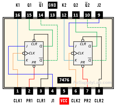
Below is the diagram for a 7476 dual J-K Flip-flop chip.
Questions
- Answer the following questions in your lab report.
- Are the flip-flops positive-edge triggered or negative-edge triggered? Explain how you know.
- Are the preset (PR) and clear (CLR) asynchronous inputs active-high or active-low? Explain how you know.
Referring to the 7476 pin assignments above, draw a wiring diagram to test the behavior of a JK flip-flop.
- Draw the logic diagram of one of the JK flip-flops (not the entire chip) and label all of the pin numbers for the inputs and outputs accordingly. (You may wish to use KiCad, in which case a power and ground table like that in Exp #10.2 is not needed.)
- In the diagram, connect the PR and CLR inputs to toggle switches, and set both inactive (again, you need to determine if connecting to power (hi) or to the ground (low) will make them inactive).
- Connect CLK to the pulser. You want the flip-flop to change state on the clock's negative edge, but you can use either pulser output (normally high or low) since either way the clock pulse has a negative edge:
or
.
- Connect the J and K inputs to two of the toggle switches and connect the Q output to an LED.
After you complete the wiring diagram, connect the circuit as shown in your diagram using the 7476 chip, a pulser (CLK), four toggle switches (J, K, PR, CLR), and an LED (Q). We assume that Q(t) and Q(t+1) will always be complements of their respective Qs, so they are not included in the table below. Also, there is no need to include a column for CLK since its use is implied in every state transition.
Table 3: State Table of JK Flip-Flop
| External Inputs | Current State | Next State | |
|---|---|---|---|
| J | K | Q(t) | Q(t+1) |
| 0 | 0 | 0 | |
| 0 | 1 | 0 | |
| 1 | 0 | 0 | |
| 1 | 1 | 0 | |
| 0 | 0 | 1 | |
| 0 | 1 | 1 | |
| 1 | 0 | 1 | |
| 1 | 1 | 1 | |
Notice: in the table that in addition to Next State there is an additional column called Current State (or called Present State). The Current State is the state of the flip-flop (Q) before the clock trigger (on the falling edge ↓ ). It is the state at time t, or Q(t). The Next State is the state of the flip-flop after the trigger; i.e. at time t+1, or Q(t+1).
Since PR and CLR affect the circuit just as they did in Exp #10.2, you would not have to test for their effects here, which is why they do not appear in this table. However, you will use them to set Current State values as shown in the table before you clock the flip-flop. Initially, connect them both to power (inactive).
Test your circuit line by line. In each case:
- Switch J and K high or low as indicated.
- Then set Current State values as shown in the table by momentarily grounding either PR or CLR (leaving the other inactive).
- Then press and release the pulser and observe Q(t+1)'s value on its LED. Enter that value into the Next State column of the table.
- For the on-campus lab, demonstrate your circuit to your instructor.
- For the online lab, take a video to demonstrate your circuit, and put the YouTube link in your report.
Exp #10.4 * Building T flip-flops from JK Flip-flops
According to Table 3, fill in the next state values in Table 4.
Table 4: State Table of J-K Flip-Flop
| External Inputs | Current State | Next State | |
|---|---|---|---|
| J | K | Q(t) | Q(t+1) |
| 0 | 0 | ||
| 0 | 1 | ||
| 1 | 0 | ||
| 1 | 1 | ||
You can build a T flip-flop from a JK flip-flop by connecting both J and K inputs together. Its diagram would be similar to that in Exp #10.3, consisting of a 7476 chip, a pulser clock (CLK), and an LED (Q). Draw the wiring diagram, but instead of separate toggle switches for J and K, including the only one which will be your T input. Connect it to both J and K.
Build a circuit and verify the result
To build and test the circuit, you would go through the table line by line, activating either PR or CLR momentarily to set Q(t) to 1 or 0 as shown in this state table. You would then toggle the T switch high or low as the table indicates. And, finally, you would pulse the clock, and then, from the Q output LED, you would fill in the Next State column.
Questions
- Here you will just fill in the Next State column into the following table based on your understanding of T-flip-flop behavior from Exp #10.1 characteristic table of T flip-flop. Then derive the equation for Q(t+1) in terms of T and Q(t).
Table 5: State Table of T Flip-Flop from the experimentDoes your circuit result table match the T flip-flop truth table?Input Current State Next State T Q(t) Q(t+1) 0 0 0 1 1 0 1 1
- For the on-campus lab, demonstrate your circuit to your instructor.
- For the online lab, take a video to demonstrate your circuit, and put the YouTube link in your report.
Exp #10.5 * Building a T flip-flop using a D Flip-flop
In a D flip-flop, the present value of its input, D(t) becomes its future output Q(t+1) after the clock trigger; i.e. Q(t+1) = D(t). So the values you placed in the column for Q(t+1) in table 4 of Exp #10.4 (above) would be the same in a column for D(t). Enter those values in table 6.
Table 6: Building a T Flip-Flop by a D Flip-Flop
| External Inputs | Current State | Flipflop Input |
|---|---|---|
| T | Q(t) | D(t) |
| 0 | 0 | |
| 0 | 1 | |
| 1 | 0 | |
| 1 | 1 |
But now the values in all three columns of the table exist at the present time--there is no future time (t+1) in this table. This transforms it into a truth table, one which describes a combinational rather than a sequential circuit (i.e. no flip-flops) and from which you can derive an equation for D in terms of T and Q.
Derive this equation and name the circuit element it describes. One of two inputs to this element is T (the other is ?) and its output goes to the D input of the flip-flop. Using KiCad to draw the wiring diagram which incorporates the D flip-flop of Exp #10.2 along with the element you just described, as well as a pulser for CLK, three toggle switches for input T, PR, CLR, and an LED for Q.
Now build the circuit and go through the state table line-by-line, entering the values for Q(t+1) as you go.
Table 7: State Table of a T Flip-Flop
| Inputs | Current State | Next State |
|---|---|---|
| T | Q(t) | Q(t+1) |
| 0 | 0 | |
| 0 | 1 | |
| 1 | 0 | |
| 1 | 1 |
Note: the clock is omitted from the table since it is understood that Q only changes when the clock triggers. PR and CLR are also omitted. You need not test their effects here — that was already done in Exp #10.2 — but you will need to use them to change the present state of Q as you go through the table.
Before you clock the flip-flop each time, first do the following:
- Switch T to the desired value shown in table 7.
- Use PR or CLR to set Q(t) to 1 or 0 as indicated in table 6. To set Q(t) to 1, momentarily ground PR then reconnect it to power (leaving CLR connected to power--inactive). To clear Q(t) to 0, momentarily ground CLR then reconnect it to power (leaving PR connected to power — inactive).
Questions
- Do your experimental results in this table agree with those you entered in the table in Exp #10.4?
- For the on-campus lab, demonstrate your circuit to your instructor.
- For the online lab, take a video to demonstrate your circuit, and write down the YouTube video link in the report.
Exp #10.6 Designing a D flip-flop using a T Flip-flop
Now, what if you wanted a D flip-flop, but only a T flip-flop and a gate are available. In this case, D would be the external input and T would be the flip-flop input. (Flip-flop output is again Q.)
Table 8: State Table of a D Flip-Flop (Using a T Flip-Flop)
| External Input | Current State | Flip-Flop Input |
|---|---|---|
| D | Q(t) | T(t) |
| 0 | 0 | |
| 0 | 1 | |
| 1 | 0 | |
| 1 | 1 |
In the table at the right, fill in values for flip-flop input T that will give the desired transitions from Q(t) to Q(t+1) required by input D. As explained at the top of Exp #10.5a, the Q(t+1) values are the same as the D values — which is why no Q(t+1) column is included. (Example: In line 2, the present value of Q(t) is 1. What should be the value of Q(t+1), and what value of T will produce it?)
Finally, derive an equation for T in terms of D and Q.
Questions
- What gate does this represent? Does it look similar to one that you've seen before?