Lab 11: Sequential Circuits
Objective
- Understand the principles of sequential circuits and how they differ from combinational logic.
- Learn to design and implement Moore and Mealy state machines.
- Build a two-bit saturating up/down counter using a Moore state machine.
- Design sequential circuits using flip-flops and logic gates.
- Experiment with practical circuits like a simple entry code detector using Moore and Mealy machines.
Required Reading Materials
- Textbook: Digital Design: with an introduction to the Verilog HDL, 5th edition, Mano and Ciletti, ISBN-13: 978-0-13-277420-8
Chapters 3 and 4 - Datasheet: 7400, 7402, 7410, 7474
Components Required
| Component/Device | Description | Quantity |
|---|---|---|
 |
Breadboard | × 1 |
| 7400 Quad 2-Input NAND Gate | ||
| 7402 Quad 2-Input NOR Gate | × 1 | |
| 7410 Triple 3-Input NAND Gate | × 1 | |
| 7474 Dual D-Type Flip-Flop | × 1 | |
| Digilent Analog Discovery 2 (AD2) or Analog Devices ADALM1000 (M1K) |
× 1 |
Experiments
Every experiment section that requires you to build a circuit and test it has an asterisk (*). For those sections:
- For the in-class lab: Demonstrate the working circuit to your lab instructor (for in-class lab)
- For online lab: Take a video to describe your circuit, upload the video to YouTube, and put the link in the report.
Exp #11.1 Saturating-Counter using Moore State Machine
As mentioned in Lab 10, sequential logic circuits are a type of logic circuit where the output of the circuit depends not only on the input, as in combinational logic circuits, but also on the sequence of past inputs that are used to determine the state of the circuit.
As we observed in Lab 10, flip-flops can be used to hold (remember) the state of the system. Each flip-flop holds one bit of data and can be used to represent one state variable within a system. A system that has N states will require log2N state variables and hence log2N flip-flops. If N is not a power of two, then you have to round log2N up to the nearest integer.
So, if you need 4 states, you will need two state variables. Let's assume that the names of the state variables are A and B. Then the four states are provided by the following values of A and B: AB = 00, 01, 10, and 11. If you need 8 states, you will need three state variables, for example, A, B, and C, where (ABC = 000, 001, 010, 011, 100, 101, 110, and 111). And if you need 6 states, you still need three state variables since log26 = 2.58 which will be 3 after rounding up (since you can’t have a fractional number of state variables). In this case, you could use any 6 of the 8 states, leaving the other 2 unused.
For example, if you had an elevator controller for a building that had floors 1 through 6, the states that indicate which floor the elevator is at would likely be 001 (1), 010 (2), 011 (3), 100 (4), 101 (5), and 110 (6), with states 000 (0) and 111 (7) unused.
Now, we are designing a two-bit saturating up/down counter. There are two output variables, A and B, and one control input X. When X = 1, the counter will count up with each clock trigger until it reaches state AB = 11 where it will remain until X is changed to 0 (i.e. the counter is saturated). Similarly, when X = 0, the counter will count down until it reaches the lowest count AB = 00, remaining until X is changed to 1. If X is changed whenever the upper or lower limit state is reached, the system will oscillate up and down from 00, 01, 10 to 11 and back.
A state diagram is used to represent the behavior of a sequential system where the state is represented by a circle, and the transitions between states are represented by an arrow (also called an edge or arc). The state diagram below represents a 2-bit saturating up/down counter.
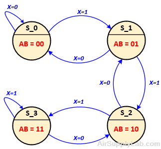
Figure 11.1: State Diagram for Moore Machine
To understand how to read a state diagram, first note that the values of X appear alongside the arrows. Next, let us consider the possible transitions from state S_1. There are two possible states: S_0 and S_2 (this can be determined by looking at the two arrows leaving state S_1). On the triggering clock edge, state S_1 will transition to state S_0 if the input X = 0 (the count goes down from 01 to 00) or transition to state S_2 if the input X = 1 (the count goes up from 01 to 10). Now, suppose it goes to state S_0. If X = 1, it will return to state S_1 on the next clock. But if X = 0, it remains in state S_0.
The block diagram below shows the overall design of a sequential circuit. The state register is built by flip-flops that are used to hold the state of the system. The flip-flop Q outputs represent the current state of the system or the present state. The state will change or transition on the triggering edge of the clock (in Lab 10, we learned that triggering can be a positive edge or a negative edge).

Figure 11.2: Sequential Circuit Architecture
In the saturating-counter example, there are four states (S_0, S_1, S_2, and S_3), so we need two bits to represent the state values. If the current state is S_1, the Q outputs for the current state will be 01, which also can be used to represent the current counter value (AB).
The combinational circuit in the diagram combines the current state-register outputs (representing the current state) with any external inputs to generate the state-register inputs that will determine the next state of the circuit at the next clock trigger. In this experiment, we use D flip-flops to store the current state. Since the next state of a D flip-flop follows the D input, the flip-flop inputs will be the same as the following state (this is not true for the other types of flip-flops, SR, JK, and T). In the saturating-counter example, if the current state is S_1 (output is AB = 01) and the input is X = 0, the next state will be S_0 (output will be AB = 00). Therefore, the following state values of inputs DADB must also equal 00. (Note: you can use any flip-flop in a sequential logic design, but the flip-flop inputs will differ depending on the type of flip-flop used.)
The saturating-counter example has one external input U but no output other than the flip-flop outputs AB (i.e. the state of the counter). The elevator example of Lab 10 is more complex: the state of the system would be the current floor that the elevator is on, the inputs would be the buttons on each floor pushed to call the elevator, and the buttons inside that select the destination floor, and the output would be used to control the motors to make the elevator go up and down. As we will see in this experiment, where the output depends on both the current state and the inputs, the circuit is called a Mealy machine. Where it depends only on the current state, it is called a Moore machine. (The elevator would be an example of the Mealy machine.)
A state table is used to design the combinational circuit within a sequential circuit. A state table differs from a truth table in that, in addition to inputs and outputs, it also represents both the current state of the system (as an input) and the next state of the system (as an output). Below is the state table for the saturating up/down counter:
| Current State (c.s) | Input | Next State (n.s) | ||||
|---|---|---|---|---|---|---|
| state | A | B | X | state | An | Bn |
| S_0 | 0 | 0 | 0 | S_0 | 0 | 0 |
| 0 | 0 | 1 | S_1 | 0 | 1 | |
| S_1 | 0 | 1 | 0 | S_0 | 0 | 0 |
| 0 | 1 | 1 | S_2 | 1 | 0 | |
| S_2 | 1 | 0 | 0 | S_1 | 0 | 1 |
| 1 | 0 | 1 | S_3 | 1 | 1 | |
| S_3 | 1 | 1 | 0 | S_2 | 1 | 0 |
| 1 | 1 | 1 | S_3 | 1 | 1 | |
Notice in the state table that the State Variables are shown twice as the current state value (before the clock trigger) and as the next state value (after the clock trigger). To design the combinational logic circuit, we need to follow these steps.
- Derive the state table based on the desired behavior of the sequential circuit (represented by the state diagram in Figure 11.1).
- Given the current and following states, based on the type of flip-flops used, determine the flip-flop inputs (since we are using D flip-flops, notice in the above table how the flip-flop inputs are the same as the following state values for states A and B).
- Derive K-maps from the state table and determine the combinational logic equations for flip-flop inputs An and Bn as a function of external input U and the present state of flip-flop outputs A and B.
- If the sequential circuit has an explicit output(s), use K-maps to determine the combinational logic equations for the outputs as a function of external input(s) and present state (for Mealy machines) or only as a function of the present state (for Moore machines).
- Draw the logic diagram with one flip-flop per state variable, the combinational logic circuits for the flip-flop inputs, and, if used, the combinational logic circuits for the circuit outputs (we do not have one in our saturating counter example).
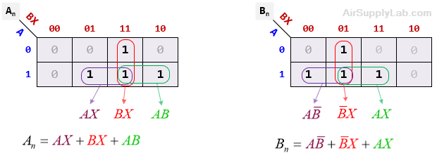
Notice that AX appears in both equations, so it is only necessary to create it once and then use it as an input to the circuit for An and for Bn.
Question
- In your lab report, copy the state table and the above equations. Next, draw the circuit diagram, including two D flip-flops (7474) and the logic circuits for An and Bn. Do not forget to include the clock input.
Exp #11.2 Sequential Circuit using Mealy State Machine
In this section, you will design (but not build) a sequential circuit, or state machine, using two D-flip-flops (7474) and some gates. This will be a "Mealy" machine; i.e. a circuit whose output is a function of both current state and inputs. The circuit has an external input X, an output Y, and two state-variable D-flip-flops A and B.
The state diagram is shown below with X/Y values along with the arrows. Because this is a Mealy machine, the output Y is determined by input X as well as by the present state AB.

Figure 11.3: Mealy State Machine Architecture
For example: alongside the arrow from state S_0 to state S_1, we see X=0 / Y=1. This means that with X=0, there will be a transition to state S_1 when the clock pulse comes. It also means that until the clock pulse comes and while the circuit is still in state S_0, the output Y will be 1 as long as X=0. Therefore, X is the current input and Y is the current output for any given current state.
-------------------------------
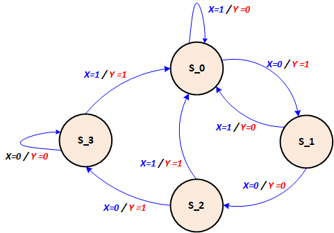
Figure 11.4: State Diagram for Mealy Machine
Table 11.1: Partially Completed State Table
| Current State | Input | Output | Next State | ||||
|---|---|---|---|---|---|---|---|
| State | A | B | X | Y | State | An | Bn |
| S_0 | 0 | 0 | 0 | 1 | S_1 | 0 | 1 |
| 0 | 0 | 1 | 0 | S_0 | 0 | 0 | |
| S_1 | 0 | 1 | 0 | 0 | S_2 | 1 | 0 |
| 0 | 1 | 1 | |||||
| S_2 | 1 | 0 | 0 | ||||
| 1 | 0 | 1 | |||||
| S_3 | 1 | 1 | 0 | ||||
| 1 | 1 | 1 | |||||
From the above state diagram, finish the state table (on your own paper). Notice in the table that each pair of rows represents the same state of AB (i.e. the same circle in the diagram).
Next, design (but do not build) the circuit. Do this with just three chips: one 7474 and 2 NAND chips. (If you need to complement A and/or B, just use inverted flip-flop outputs — there is no need to use gates as inverters. But you will need a gate to produce X .)
Questions
For this experiment:
- From the state table, derive maps for An, Bn, and Y from the maps, and derive their equations. Each map is labeled as shown. Since A's column in the state table is at the left, it appears at the bottom row of the map.
BX
A
00 01 11 10 0 1 An =
BX
A
00 01 11 10 0 1 Bn =
BX
A
00 01 11 10 0 1 Y =
- Draw the circuits using only a 7474 (dual D flip-flops) and NANDs (7400's and/or 7410's, but no 7408's or 7432's). Use DeMorgan symbols for NANDs but only where doing so preserves the original AND/OR structure. A diagram with all normal or all DM gate symbols is not acceptable. (Remember: connecting wires must either have bubbles at both ends or no bubbles at all.)
Exp #11.3 * Build a Moore State Machine Circuit
This section is similar to Exp#11.2 except that the sequential circuit here is a "Moore" machine — a state machine whose output depends only on the current state, not on inputs. The circuit has two D-flip-flops, A, B, an input X (from a switch), and an output Y (connected to an LED). Its state diagram is shown below.

Figure 11.5: More State Machine Architecture
You can think of this circuit as a primitive entry-code detector. You enter a sequence of values for input X and move the circuit from state to state. (This would be like pressing a sequence of keys in a special order to gain entry to a room, a car, or whatever.)
Here, each step involves setting input X to 0 or 1 (using a switch) and then pressing a pulser. You do this at least 3 times. If you set X to the right value each time, the state machine reaches state 3 (AB = 11). At this time, Y goes high and turns on its LED, indicating that you have gained entry. If at any point, you clock in a wrong value for X, the state machine returns to 0 where you have to try a new sequence for X.
Of course, with a real entry-code detector, if you did not know the code there would be too many possible sequences to try — here there are only 8. Also, unlike here, just pressing a key enters it; you do not have to clock it in with a pulser.
In the state diagram, you see values for X alongside the arrows, labeled X0, X1, and X2. They represent the sequence of numerical values (0's and 1's) for X that are required to get you to state 3. You will choose a sequence for your circuit. As the state diagram shows, if the complement of any required Xn (i.e. Xn) is entered, the circuit returns to S_0 (AB = 00) and waits for a new sequence to begin. Notice that once in the state S_3, the next state is S_0, regardless of X's value.
In a Moore machine, output Y is not dependent on X as it was in the Mealy machine; it depends only on the current state of the circuit S_n (AB). This is why it is placed under the state number inside the state circle, not alongside the arrows. So, in states S_0, S_1, and S_2, Y = 0, indicating that the required sequence of X's is not yet complete. When it is, Y = 1, which turns on an LED to signal that the key code was successfully entered.
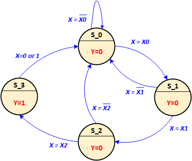
Figure 11.6: State Diagram for Moore Machine
Design steps:
- Choose a sequence of values for X. Make X2 the same as X0 (X0 = 0, X2 = 0 or X0 = 1, X2 = 1) and make X1 the opposite. Example: X0 = 0, X2 = 0, so X1 = 1, or the opposite. (This may simplify the circuit you will build.)
X0 = X1 = X2 = - Derive the state table from Figure 11.6 state diagram. The table has the same format as that in Exp# 11.2.
Current State Input Output Next State State A B X Y State An Bn S_0 0 0 0 0 0 1 S_1 0 1 0 0 1 1 S_2 1 0 0 1 0 1 S_3 1 1 0 1 1 1 - From the table, draw K-maps for An, Bn, and Y, and from the maps, and derive equations in their simplest form.
BX
A
00 01 11 10 0 1 An =
BX
A
00 01 11 10 0 1 Bn =
BX
A
00 01 11 10 0 1 Y =
- Use KiCad to draw the circuit. Only three chips are needed: a 7474 (dual D-flip-flops), a 7410 (NAND), and a 7402 (NOR). Do not use a 7400. Remember: a 7410 NAND gate can also be drawn as an invert-OR and a 7402 NOR gate can also be drawn as an invert-AND. Use DeMorgan symbols where appropriate. Inverters are not needed for A and B since they are available as flip-flop outputs.
- Build the circuit. Bring state variables A and B as well as Y to LEDs so you can monitor the sequence of states and the output.
Start by momentarily grounding the clear inputs of both flip-flops to put the circuit into state 0. Then,
- Set X to X0 and clock the circuit with a pulser. The state should remain at S_0.
- Repeat with X = X0. The state should move to S_1.
Repeat this test method, moving to the next state by entering the correct subsequence to get there. Then enter X for that state and return to S_0. Continue until you have checked all the states. (Of course, from state S_3 you can only go back to S_0 — there is no correct or incorrect value for X.)
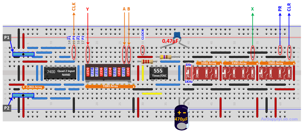
- For the on-campus lab, have your instructor check your results.
- For the online lab, take pictures for each input step, and post them in the report.
Exp# 11.4 Mealy State Machine
Mealy example: Table 2 is similar to but not the same as the one in Exp #11.3. The values of Y depend on state variables A and B and on input X, not just on A and B (see the first two rows as an example). So this represents a Mealy machine.
Table 2: State Table
| Current State | Input | Output | Next State | ||||
|---|---|---|---|---|---|---|---|
| State | A | B | X | Y | State | An | Bn |
| S_0 | 0 | 0 | 0 | 1 | S_1 | 0 | 1 |
| 0 | 0 | 1 | 0 | S_0 | 0 | 0 | |
| S_1 | 0 | 1 | 0 | 0 | S_2 | 1 | 0 |
| 0 | 1 | 1 | 1 | S_3 | 1 | 1 | |
| S_2 | 1 | 0 | 0 | 1 | S_1 | 0 | 1 |
| 1 | 0 | 1 | 0 | S_0 | 0 | 0 | |
| S_3 | 1 | 1 | 0 | 1 | S_3 | 1 | 1 |
| 1 | 1 | 1 | 0 | S_2 | 1 | 0 | |
Table 3: Truth Table
| Current State | Input | Next State | ||
|---|---|---|---|---|
| A | B | X | An | Bn |
| 0 | 0 | 0 | 0 | 1 |
| 0 | 0 | 1 | 0 | 0 |
| 0 | 1 | 0 | 1 | 0 |
| 0 | 1 | 1 | 1 | 1 |
| 1 | 0 | 0 | 0 | 1 |
| 1 | 0 | 1 | 0 | 0 |
| 1 | 1 | 0 | 1 | 1 |
| 1 | 1 | 1 | 1 | 0 |
Since the values of Y in each row exist at the same time as the corresponding values of A, B, and X (i.e. all in the present state), then the first 4 columns (shaded) can be treated as a simple truth table, and we can design a circuit for Y using gates but no flip-flops. (You would just fill in an 8-square K-map.)
Here we omit Y in Table 3 to concentrate on An and Bn. Using D flip-flops simplifies the next-state design. The D values are the same as the n.s. values since at the triggering edge of the clock, the D values are stored into the flip-flops and emerge as the new A and B. Since the D's exist at the same time as A, B (current state), and X, we can design circuits for them using K-maps, just like for Y.
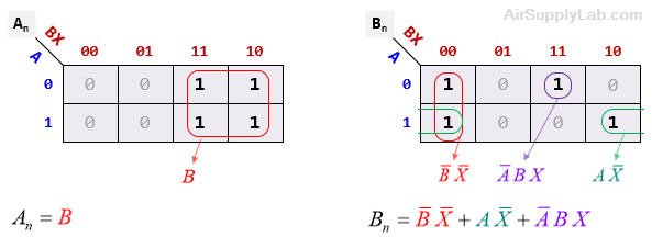
Figure 11.7: K-Map for Next State
From the K maps of Figure 11.7, we derive expressions for the flipflop inputs:
An = B
Bn = B X + A X + A B X
Now, suppose you build circuits for An and Bn and connect them to their flip-flops' inputs. You then supply pulses to the flipflop CLK inputs and also input a series of values for X, synchronized with the clock.
The diagrams in Figure 11.8 below demonstrate the behavior of the circuit as it responds to the clock pulses. The result is a sequence of states over time representing the dynamic behavior of the circuit for a particular series of input X values.
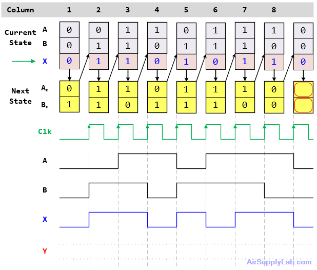
Figure 11.8: Timing Diagram of the Circuit
At the start of each present state, the circuit uses values of flip-flops A and B and an input X to generate An and Bn. This is indicated by the down arrows in the diagram. Thus, A, B, X, An, and Bn all exist at the same time. Then, when the clock pulse comes, An and Bn values are moved into their respective flip-flops and become the next present state of A and B as indicated by the up arrows. At the same time, a new value is supplied to X.
The waveforms shown below indicate how A and B change from state to state as input X assumes various values over time (assigned here at random). This illustrates the dynamics of state machine behavior.
Question
- Based on Table 2, use the online diagram website (https://app.diagrams.net/) to draw the state diagram, and post it in your report.
- Assume that X will equal 0 after the final clock pulse. What will be the new values of An and Bn? (Include the answer in Exp# 11.1.)
Finally, suppose output Y was included in the circuit. In Figure 11.8 it would appear at the bottom of each column along with outputs An and Bn. Now consider the cases where A and B are the same but X is not; e.g. columns 3 and 6 (or 4 and 8). In a Moore circuit, Y depends only on A and B and not on X, so the value of Y in both columns would be the same. But in a Mealy circuit, Y depends as well on X, so its value could change.
- Draw the state of the signal Y on the timing diagram in Figure 11.8.