Page 14 - EE2449_TTL_Datasheet
P. 14

SN54/74LS74A
             DUAL D-TYPE POSITIVE
             EDGE-TRIGGERED FLIP-FLOP


               The SN54/74LS74A dual edge-triggered flip-flop utilizes Schottky TTL cir-
             cuitry to produce high speed D-type flip-flops. Each flip-flop has individual
             clear and set inputs, and also complementary Q and Q outputs.          DUAL D-TYPE POSITIVE
               Information at input D is transferred to the Q output on the positive-going  EDGE-TRIGGERED FLIP-FLOP
             edge of the clock pulse. Clock triggering occurs at a voltage level of the clock
                                                                                    LOW POWER SCHOTTKY
             pulse and is not directly related to the transition time of the positive-going
             pulse. When the clock input is at either the HIGH or the LOW level, the D input
             signal has no effect.


                                                                                                    J SUFFIX
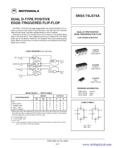
                             LOGIC DIAGRAM (Each Flip-Flop)                                         CERAMIC
                                                                                                   CASE 632-08
                                                                                 14
                                                                                     1
                 SET (S D )
                      4 (10)
                                                                    Q
                                                                  5 (9)
               CLEAR (CD)
                      1 (13)                                                                        N SUFFIX
                                                                                                    PLASTIC
                  CLOCK                                                           14               CASE 646-06
                      3 (11)
                                                                    Q               1
                                                                  6 (8)
                     D
                      2 (12)
                                                                                                    D SUFFIX
                                                                                                      SOIC
                                                                                    14
                                                                                        1         CASE 751A-02


                                                                                    ORDERING INFORMATION
                                                                                     SN54LSXXJ   Ceramic
                             MODE SELECT — TRUTH TABLE                               SN74LSXXN   Plastic
                                                                                     SN74LSXXD   SOIC
                                             INPUTS           OUTPUTS
                 OPERATING MODE
                 OPERA TING   MODE
                                       S D    S D     D      Q      Q
              Set                       L      H      X      H       L                  LOGIC SYMBOL
              Reset (Clear)             H      L      X      L      H
              *Undetermined             L      L      X      H      H                   4              10
              Load “1” (Set)            H      H      h      H       L
              Load “0” (Reset)          H      H      l      L      H                  S D             S D
                                                                                 2   D    Q   5  12  D    Q  9
             * Both outputs will be HIGH while both S D  and C D  are LOW, but the output states are unpredictable
              if S D  and C D  go HIGH simultaneously. If the levels at the set and clear are near V IL  maximum then  3  CP  11  CP
              we cannot guarantee to meet the minimum level for V OH .
             H, h = HIGH Voltage Level                                                    Q   6           Q  8
                                                                                       C D             C D
             L, I = LOW Voltage Level
             X = Don’t Care
             i, h (q) = Lower case letters indicate the state of the referenced input (or output) one set-up time  1  13
             i, h (q) = prior to the HIGH to LOW clock transition.
                                                                                           V CC  = PIN 14
                                                                                           GND = PIN 7


                                                    FAST AND LS TTL DATA
                                                             5-71
                                                                                          www.AirSuplyLab.com
                                                                                          www.AirSuplyLab.com
   9   10   11   12   13   14   15   16   17   18   19