Page 36 - EE2449_TTL_Datasheet
P. 36

SN54/74LS155
           DUAL 1-OF-4 DECODER/                                                  SN54/74LS156

           DEMULTIPLEXER

             The SN54/74LS155 and SN54/74LS156 are high speed Dual 1-of-4
           Decoder/Demultiplexers. These devices have two decoders with common
           2-bit Address inputs and separate gated Enable inputs. Decoder “a” has an  DUAL 1-OF-4 DECODER/
           Enable gate with one active HIGH and one active LOW input. Decoder “b” has
           two active LOW Enable inputs. If the Enable functions are satisfied, one  DEMULTIPLEXER
           output of each decoder will be LOW as selected by the address inputs. The  LS156-OPEN-COLLECTOR
           LS156 has open collector outputs for wired-OR (DOT-AND) decoding and
                                                                                   LOW POWER SCHOTTKY
           function generator applications.
             The LS155 and LS156 are fabricated with the Schottky barrier diode
           process for high speed and are completely compatible with all Motorola TTL
           families.
           • Schottky Process for High Speed
                                                                                                  J SUFFIX
           • Multifunction Capability                                                             CERAMIC
           • Common Address Inputs                                                               CASE 620-09
                                                                                16
           • True or Complement Data Demultiplexing
                                                                                   1
           • Input Clamp Diodes Limit High Speed Termination Effects
           • ESD > 3500 Volts

                                                                                                  N SUFFIX
                                                                                                   PLASTIC
                                                                                                 CASE 648-08
                                                                                16
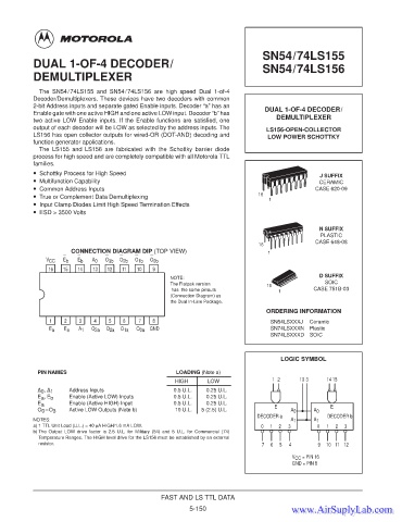
                       CONNECTION DIAGRAM DIP (TOP VIEW)                           1
               V CC  E b  E b  A 0  O 3b  O 2b  O 1b  O 0b
                16  15   14  13   12  11   10   9
                                                                                                  D SUFFIX
                                                     NOTE:
                                                     The Flatpak version                            SOIC
                                                                                  16
                                                      has  the same pinouts           1          CASE 751B-03
                                                     (Connection Diagram) as
                                                     the Dual In-Line Package.
                                                                                  ORDERING INFORMATION
                1    2   3    4   5   6    7    8                                  SN54LSXXXJ  Ceramic
                E a  E a  A 1  O 3a  O 2a  O 1a  O 0a  GND                         SN74LSXXXN  Plastic
                                                                                   SN74LSXXXD  SOIC


                                                                                       LOGIC SYMBOL
            PIN NAMES                                  LOADING (Note a)
                                                      HIGH      LOW                 1 2     13 3     14 15
            A 0 , A 1  Address Inputs                 0.5 U.L.  0.25 U.L.
            E a , E b  Enable (Active LOW) Inputs     0.5 U.L.  0.25 U.L.
            E a       Enable (Active HIGH) Input      0.5 U.L.  0.25 U.L.
                                                                                     E                E
            O 0 –O 3  Active LOW Outputs (Note b)     10 U.L.  5 (2.5) U.L.               A 0    A 0
                                                                               DECODER a             DECODER b
           NOTES:                                                                         A 1    A 1
           a) 1 TTL Unit Load (U.L.) = 40 mA HIGH/1.6 mA LOW.                    0  1  2  3       0  1  2  3
           b) The Output LOW drive factor is 2.5 U.L. for Military (54) and  5  U.L.  for  Commercial  (74)
             Temperature Ranges. The HIGH level drive for the LS156 must be established by an external
             resistor.                                                           7  6  5  4       9  10 11 12
                                                                                          V CC  = PIN 16
                                                                                          GND = PIN 8


                                                  FAST AND LS TTL DATA
                                                           5-150
                                                                                          www.AirSuplyLab.com
                                                                                          www.AirSuplyLab.com
   31   32   33   34   35   36   37   38   39   40   41